
Products
Thick Film Printed Cu Substrate (TPC)
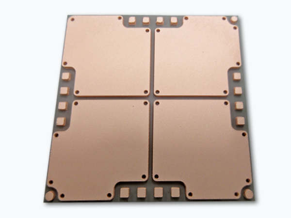
By screen printing our copper pastes onto various substrates, including ceramic substrates, thick-film copper patterns can be formed.
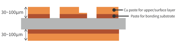
The design flexibility of the printing pattern also enables the formation of stepped structures, making it possible to achieve copper thicknesses suitable for power device applications.
Furthermore, the bonding reliability to various ceramic substrates is comparable to that of AMB (Active Metal Brazed) substrates, providing excellent durability and long-term stability.
Features
-
Compatible with Various Substrates
Compatible with a wide range of ceramic substrates, including silicon nitride (Si₃N₄), aluminum nitride (AlN), sapphire, and alumina (Al₂O₃).By utilizing copper paste lamination technology based on the screen-printing process, uniform and stable thick-film copper wiring can be formed even on high-hardness, highly insulating ceramic substrates that are difficult to process using conventional direct bonding technologies.
-
Flexible Thickness ControlThe lamination of copper paste by screen printing enables stepwise control of copper thickness through mask design and optimization of the number of printing cycles, allowing stepped structures to be formed with ease.
Specification
| Reference standard | Remarks | ||
|---|---|---|---|
| Base material | Material | AlN, Al₂O₃, SiN | Other materials on request |
| Size | 50~114 mm□ | - | |
| Thickness | 0.2 mm | - | |
| Conductive property | L/S | ≧ 300 / 300 μ | - |
| Film thickness | 30〜100 μ | 100μ or more on request | |
| Resistivity | 2.5~5.0 μΩcm | - | |
| Adhesion before plating | ≧3.0 kgf / 2mm□ | Measured by peel test | |
| Adhesion after plating | ≧2.5 kgf / 2mm□ | Measured by peel test | |
Application
-
Ceramic heat dissipation circuit packages for power devices, etc.