
Products
Via-filling Substrate
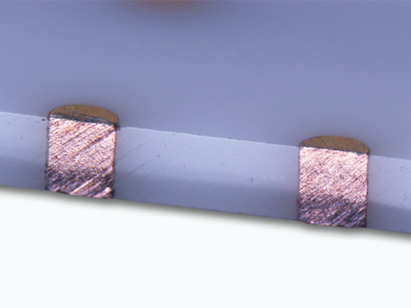
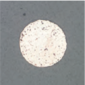
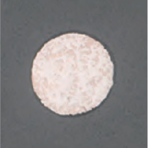
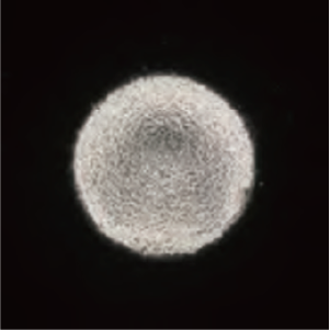
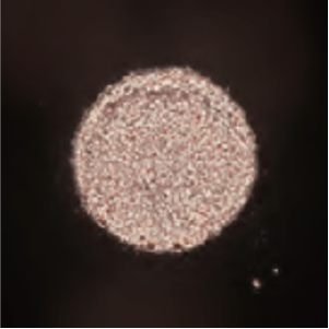
By employing a high-conductivity, non-shrinkage via-filling process, copper paste or silver paste can be uniformly filled into a wide variety of via structures.
This technology has been widely adopted in ceramic packages for telecommunications applications and has earned a strong reputation for high reliability and consistent quality.
We supply these products as via-filled semi-finished substrates and provide a comprehensive service covering via drilling, via filling, and polishing.
By offering a one-stop process solution, we help simplify process management and ensure consistent product quality.
Features
-
Highly Reliable and High-Performance Via-Filled Structures
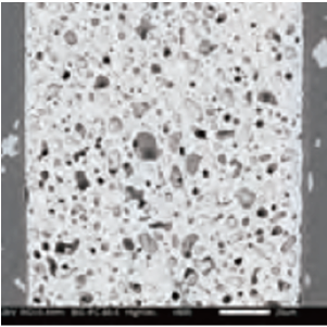
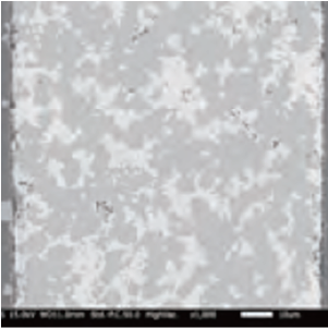
Uniform via filling with minimal voids and gaps provides excellent adhesion to the substrate. These structures offer outstanding electrical and mechanical reliability and are suitable for applications requiring high-density wiring and high heat dissipation performance. -
Smooth Substrate Surface for Improved Mountability
The substrate surface can be finished to a high degree of flatness, enabling component mounting directly above filled vias. This increases design flexibility and allows more efficient utilization of substrate space. -
Compliance with Environmental Regulations
Compliant with the RoHS 2 Directive, these materials can be used with confidence while helping to reduce environmental impact.
Specification
| Item | Ceramic substrate | Glass substrate | Organic substrate | ||||
|---|---|---|---|---|---|---|---|
| Substrates | Substrate Material | AlN, Al₂O₃, SiN | Quartz glass, Alkali-free glass | Glass epoxy | |||
| Size, Thickness | 2×2~4.5×4.5 inch, 0.2~1.0 mm | 2×2~4.5×4.5 inch, 0.2~1.0 mm | 2×2~4.5×4.5 inch, 0.2~1.0 mm | ||||
| Via | Filled Metal | Ag | Cu | Ag-Cu alloy | Ag | Cu | Ag |
| Via Diameter | Φ0.05~1.0 mm | Φ0.05~2.0 mm | Φ0.05~1.0 mm | Φ0.05~0.5 mm | Φ0.05~0.5 mm | Φ0.05~0.5 mm | |
| Firing Temperature | ~900 ℃ | ~900 ℃ | ~900 ℃ | 500~600 ℃ | 400~800 ℃ | 200~300 ℃ | |
| Firing Atmosphere | Air | N₂ | N₂ | Air | N₂ | Air | |
| Specific Resistivity | 3~4 µΩ・cm | 5~7 µΩ・cm | 10 µΩ・cm | 2~4 µΩ・cm | 3~6 µΩ・cm | 5~8 µΩ・cm | |
| Aspect Ratio | 1.0~10.0 | 1.0~10.0 | 1.0~6.5 | 1.0~10.0 | 1.0~10.0 | 1.0~10.0 | |
| Non-polished | Flatness of filled area | <±30 µm | <±30 µm | - | <±20 µm | <±20 µm | <±20 µm |
| LAP polishing | Recommended Polishing Allowance* |
>0.15 mm | >0.15 mm | >0.15 mm | >0.15 mm | >0.15 mm | >0.15 mm |
| Flatness of filled area | <±3 µm | <±3 µm | <±3 µm | <±3 µm | <±3 µm | <±3 µm | |
| POL polishing | Recommended Polishing Allowance* |
>0.15 mm | >0.15 mm | >0.15 mm | >0.15 mm | >0.15 mm | >0.15 mm |
| Flatness of filled area | <±2 µm | <±2 µm | <±2 µm | - | - | - | |
| Via cross-section | 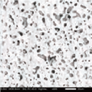 |
 |
 |
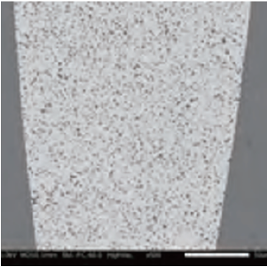 |
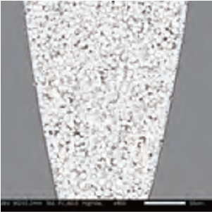 |
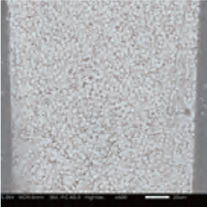 |
|
| Via surface | 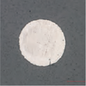 |
 |
 |
 |
 |
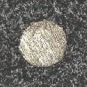 |
|
*The value shown in column is the sum of both sides of the substrate.
Application
-
Package Substrates and Module Substrates Requiring High Reliability and Efficient Heat Dissipation