![]()
-
About Us
-
Investor Relations
- Sustainability
-
Products
- Products TOP
- Field of Application
- Automobile and Motorcycle Transmission Belts and Related Products
- Industrial Power Transmission Belts and Related Products
- Conveyor Belts, Systems and Related Products
- Engineering Plastics Materials and Processed Products
- Waterproofing Materials for Construction and Related Products
- Civil Engineering Water-shielding Materials
- Electronic Materials and Coating Materials
- Other Products
- Catalog
-
Technical Support
- Resources Library
-
Global Group Sites
_eng.png)
Products
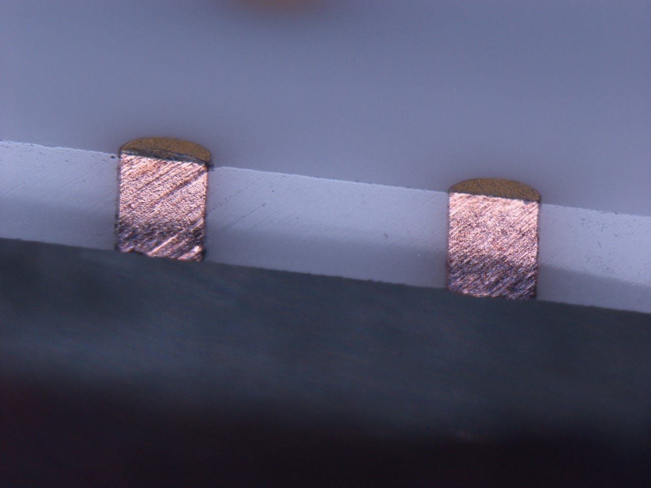
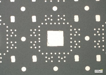
Cu Substrate with filled via
The high-conductivity, no-shrinkage filling method using Mitsuboshi's proprietary copper paste formula enables uniform filling of a variety of vias. Our products have been used in many telecommunication-related ceramic packages that require high reliability, and we have an established reputation for high quality.
* Sold as semi-processed ceramic substrates with via filling process. We offer a wide range of services including drilling, via filling, and polishing, and can also provide batch processing.
Features
・High reliability, high densification, high heat dissipation
・RoHS2 compliant
・customizable
・high adhesion to substrates
・ smooth surface finish on substrates, and mounting of components directly above filled vias possible.
Uniform via filling with few voids and gaps is possible.
・High airtightness with minimized voids and gaps is also available (Consult with us).
Achievement
・Filling is possible for high-aspect-ratio holes, large-diameter holes, mixed holes of different diameters, and irregular shapes.
The filled part has high thermal conductivity and can be used as a thermal via.
(Filling of quartz and sapphire substrates with low dielectric loss at high frequencies (in the GHz range) is possible.
Noise can be suppressed by shortening the wiring length.
・Highly dense via processing with high gas barrier properties is also available. (Consult with us).
Achievement・Assumed Applications
・Various package substrates and module substrates that require high reliability and heat dissipation
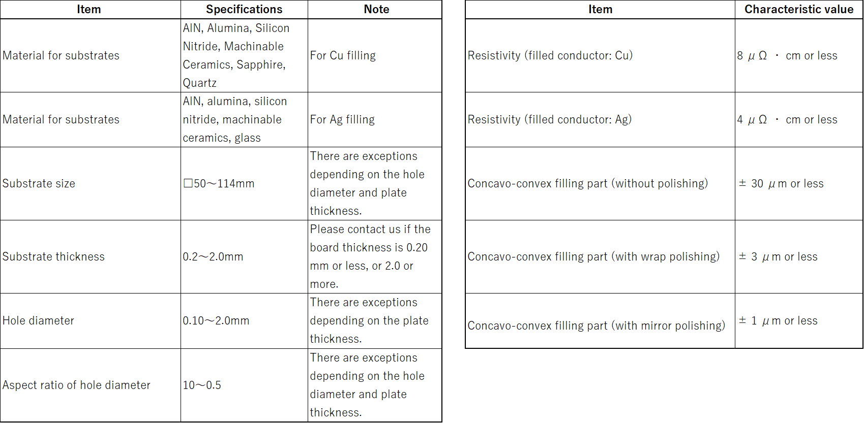
specification
Precautions
・The above data and specifications are examples.
Remarks
・Please contact us for consultation on via filling using pastes other than copper (Mainly silver).
©2022 Mitsuboshi Belting Ltd. All Rights Reserved.